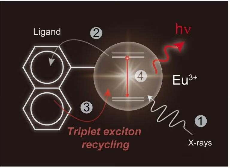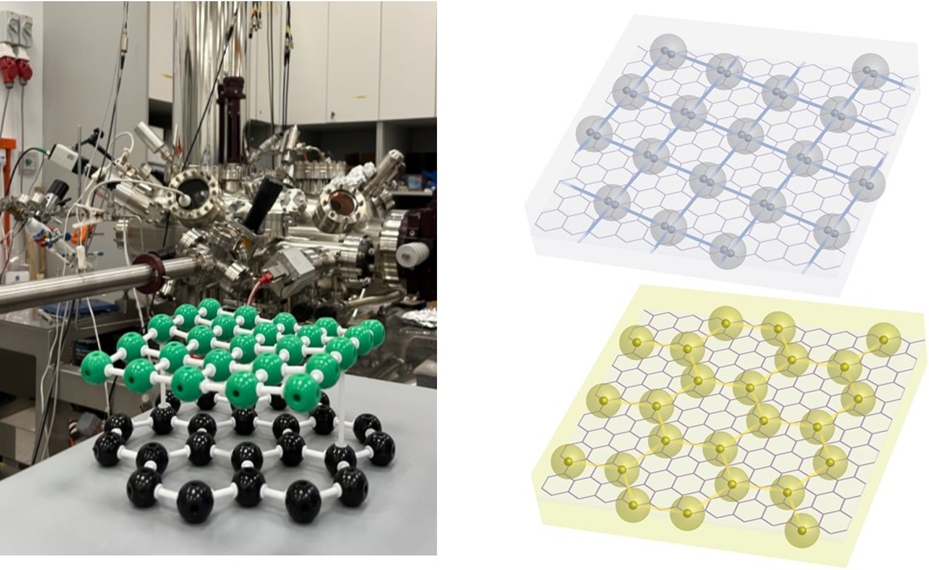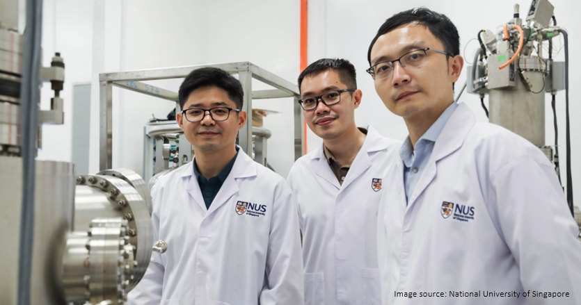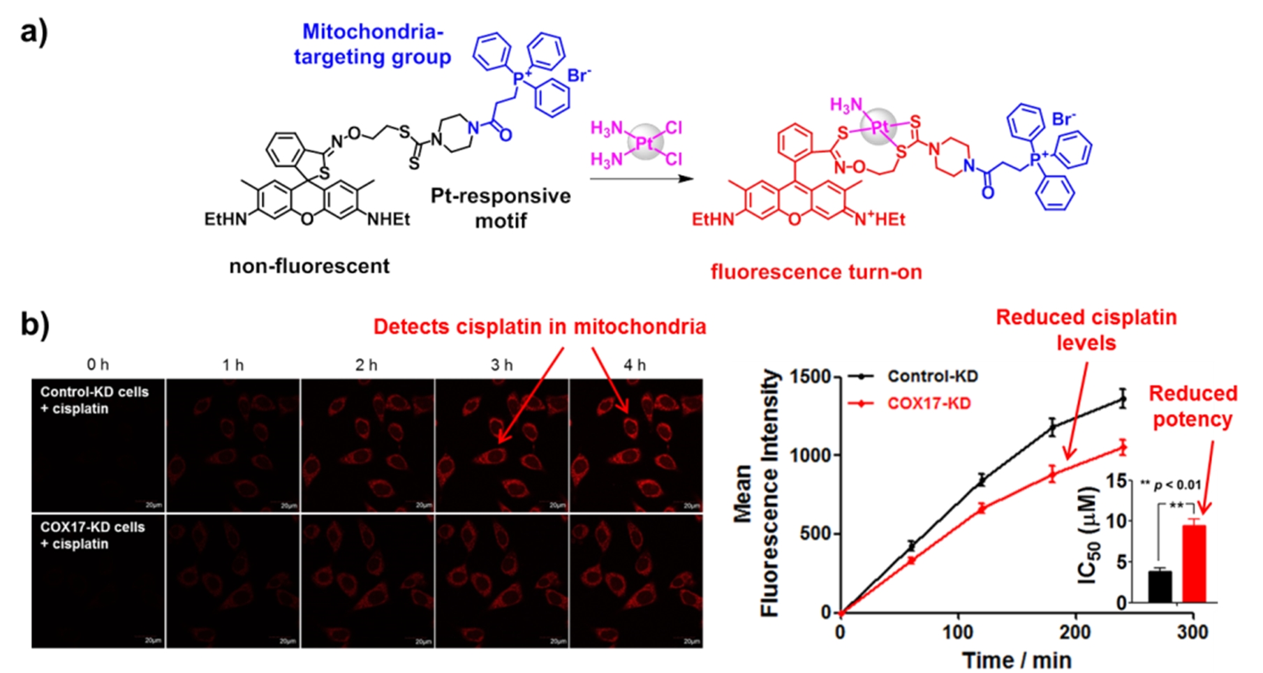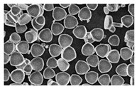
A research team led by Professor CHEN Wei from the Department of Physics and the Department of Chemistry at NUS, synthesized single-layer semiconducting Cr2Se3 and demonstrated the CDW phenomenon using scanning tunnelling microscopy (STM). Contrary to the previously reported 2D metallic TMCs, CDW in semiconducting Cr2Se3 can be cleanly and reversibly tuned via surface charge transfer doping, without introducing foreign impurities. This research work was carried out in collaboration with Professor ZHENG Feipeng from Jinan University, China.
The research findings were published in the scientific journal Science Advances.
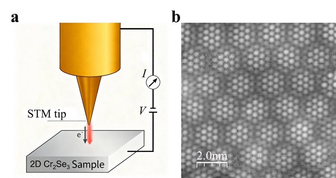
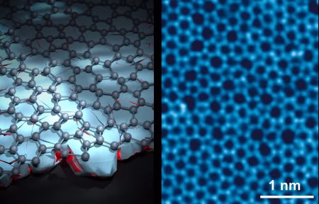
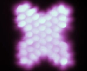
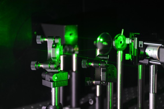
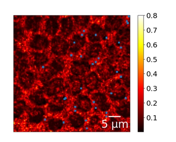
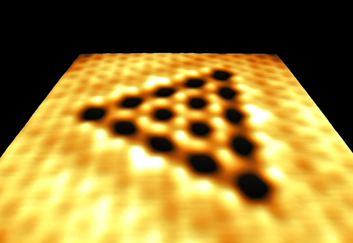
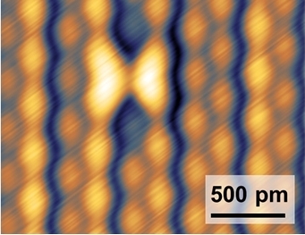
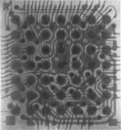
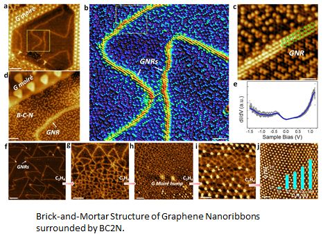
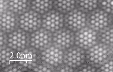
Figure shows (a) schematic diagram of the scanning tunnelling microscopy (STM) measurement on two-dimensional (2D) Chromium (III) selenide (Cr2Se3). (b) High resolution STM image revealing the granular charge density wave (CDW) pattern in 2D Cr2Se3.
One of the authors, Dr DUAN Sisheng said, “Due to its semiconducting nature, the CDW in 2D Cr2Se3 can be tuned through both electron and hole doping. This suggests potential device applications for extrinsic manipulation of electronic correlated phases.” “In fact, 2D Cr2Se3 is also antiferromagnetic. A doping tunable CDW in a 2D antiferromagnet offers a platform for understanding the interplay between magnetism, charge order, and electron correlation,” added Professor Chen. Read the full article here.